Ethernet on an FPGA sounds like one of those projects that begins with confidence and ends with a person staring at a timing diagram at 2:13 a.m., whispering, “Why is this nibble backwards?” But the good news is that Ethernet is not magic. It is a very disciplined parade of bits, bytes, clocks, checksums, addresses, and tiny rules that punish assumptions with the emotional precision of a compiler error.
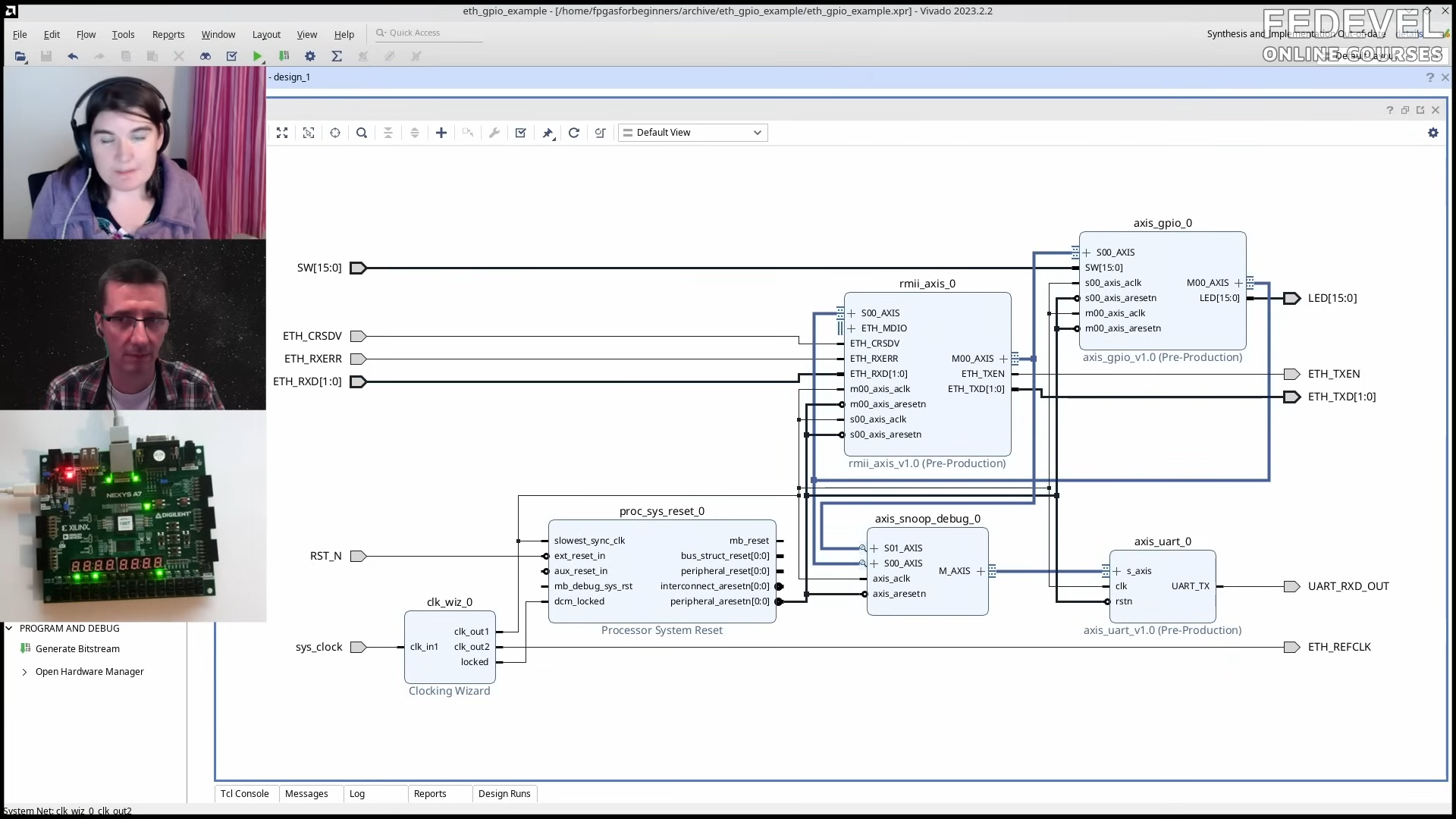
This guide is for builders who want to understand FPGA Ethernet at a low level instead of simply dropping in a vendor IP block, clicking “generate,” and hoping the blinking link LED means victory. Vendor cores are useful, but learning what happens underneath them gives you sharper debugging instincts, better performance control, and fewer moments where your board behaves like a moody toaster with an RJ45 jack.
At the lowest practical level, doing Ethernet on an FPGA means building or integrating logic that can talk to a physical Ethernet transceiver, create valid Ethernet frames, recognize incoming frames, handle timing, and optionally climb the network stack into ARP, IPv4, UDP, or TCP. For many FPGA projects, UDP over Ethernet is the sweet spot: fast, simple, predictable, and much easier than implementing a full TCP stack from scratch.
What “Ethernet on an FPGA” Actually Means
An FPGA does not usually connect directly to the copper wires in an Ethernet cable. That job belongs to the PHY, short for physical layer transceiver. The PHY handles electrical signaling, line coding, cable negotiation, magnetics, and other analog-ish chores that digital designers are happy to delegate. The FPGA usually implements the MAC side: it sends and receives frames, manages clocks and control signals, checks frame boundaries, calculates CRC values, and decides what to do with the payload.
The common architecture looks like this: your application logic feeds data into a packet builder, the packet builder creates an Ethernet frame, the MAC sends that frame through an interface such as MII, RMII, GMII, RGMII, or SGMII, and the PHY turns it into actual signals on the cable. On receive, the process runs backward. The PHY recovers data from the wire, the FPGA captures it, the MAC validates it, and your packet parser decides whether the frame is useful or digital confetti.
The Basic Building Blocks
1. The PHY
The PHY is the chip near the Ethernet jack. It negotiates link speed, handles the physical medium, and provides a digital interface to the FPGA. For 10/100 Mbps Ethernet, you may encounter MII or RMII. For Gigabit Ethernet, GMII and RGMII are common. Higher-speed designs often move toward SGMII, XGMII, or transceiver-based interfaces.
A beginner-friendly FPGA Ethernet project often starts with a board that already has an RJ45 connector and PHY installed. This saves you from the joys of controlled impedance routing, magnetics layout, and trying to determine whether your failed packet transmission is caused by HDL, clocks, or a PCB trace that has chosen a career in abstract art.
2. The MAC
The MAC, or Media Access Control block, is where your FPGA becomes a proper Ethernet citizen. It forms transmit frames, detects receive frames, handles preamble and start-of-frame delimiter behavior, enforces minimum frame sizes, manages interpacket gap timing, and calculates or checks the Ethernet frame check sequence.
You can use a vendor MAC core, an open-source MAC, or write a minimal MAC yourself. Writing a basic transmit-only MAC is not impossible. Writing a robust, reusable, production-grade MAC that handles every corner case is a larger beast. It is less “weekend project” and more “weekend project that quietly steals several more weekends.”
3. The Interface Between MAC and PHY
The FPGA talks to the PHY using a defined interface. MII uses separate transmit and receive clocks and four-bit data paths for 10/100 Mbps operation. RMII reduces pin count by using a two-bit data path and a shared reference clock. GMII uses an eight-bit data path at 125 MHz for Gigabit Ethernet. RGMII reduces the GMII pin count by transferring four bits on both clock edges, which is efficient but more timing-sensitive.
RGMII is popular because it saves pins, but it demands respect. Data is double data rate, clock-to-data skew matters, and constraints must be correct. If the design almost works, randomly fails, or only behaves when you glare at it, suspect timing first. Ethernet is many things, but forgiving of sloppy clocking is not one of them.
The Ethernet Frame: Your First Real Packet
A standard Ethernet II frame contains a destination MAC address, a source MAC address, an EtherType field, payload data, and a frame check sequence. On the wire, the packet is preceded by a preamble and start frame delimiter. The preamble is typically seven bytes of 0x55, followed by the start frame delimiter 0xD5. That pattern helps the receiver synchronize before the real frame begins.
The frame itself begins with six bytes of destination MAC address. If you are sending to one known computer on a direct cable, this can be the computer’s MAC address. If you are broadcasting an ARP request, the destination is FF:FF:FF:FF:FF:FF. Next comes the six-byte source MAC address, which is the address you assign to your FPGA design. Then comes the EtherType. For IPv4, that value is 0x0800. For ARP, it is 0x0806.
The minimum Ethernet frame size from destination MAC through FCS is 64 bytes. Since the header is 14 bytes and the FCS is 4 bytes, the payload must be padded when needed. This is one of the classic “why does Wireshark show something weird?” moments. Your payload may be short, but Ethernet still expects the frame to meet the minimum size. The network does not care that your test message was only “hi.” It wants its padding, thank you very much.
Start Simple: Transmit One Raw Ethernet Frame
The simplest useful FPGA Ethernet experiment is transmitting a fixed Ethernet frame over and over. You do not need ARP, IP, UDP, DHCP, or a heroic software stack. You can hard-code the destination MAC address of your PC, assign a fake but locally unique source MAC address to the FPGA, choose a custom EtherType, and send a payload with recognizable bytes.
On the PC side, use a packet capture tool such as Wireshark. If your frame appears, celebrate. You have successfully convinced an FPGA to speak Ethernet at layer 2. That is not a small thing. Somewhere inside the board, flip-flops are wearing tiny party hats.
A minimal transmit state machine usually includes states for idle, preamble, SFD, destination MAC, source MAC, EtherType, payload, padding if required, FCS, and interpacket gap. The exact implementation depends on the PHY interface. On an eight-bit GMII-style interface, you send one byte per clock. On a four-bit MII or RGMII-style path, you must handle nibbles and edge timing correctly.
CRC: The Part Everyone Tries To Ignore
The Ethernet frame check sequence is a 32-bit CRC. It detects transmission errors and is required for valid frames. During early experiments, some PHY or MAC cores may generate the FCS for you. If you are building the MAC yourself, you must generate it correctly.
CRC bugs are especially annoying because everything else can look right. The destination MAC is right. The payload is right. The waveform looks right. Then the receiving device silently discards the frame because the FCS is wrong. Ethernet hardware does not send you a comforting note. It just drops the frame and moves on with its life.
The practical advice is simple: use a known-good CRC implementation, test it against known Ethernet frame examples, and verify byte ordering carefully. CRC logic in HDL is not conceptually impossible, but bit order and initialization values matter. This is where many otherwise sane engineers briefly become philosophers.
Receiving Frames: Where Reality Enters The Chat
Transmit-only Ethernet is fun, but receive support makes the FPGA interactive. A receive path must detect the start of a frame, collect bytes, check destination address, identify EtherType, buffer or stream payload data, verify CRC, and recover cleanly after bad frames.
The receive logic should not assume that every incoming frame is for your FPGA. Networks are noisy places. Even a quiet LAN may contain broadcasts, ARP requests, IPv6 neighbor discovery packets, multicast traffic, and other frames your design does not understand. Your parser should quickly reject irrelevant frames and avoid getting stuck when malformed data appears.
A good receive design is built as a pipeline. First, capture symbols or bytes from the PHY interface. Next, align the frame and locate the SFD. Then parse header fields. Then route the payload to ARP, IPv4, UDP, or a custom protocol handler. Finally, check the FCS or rely on the MAC layer to report whether the frame was valid.
Why ARP Matters
If you want your FPGA to send IPv4 packets to a PC without hard-coding the PC’s MAC address, you need ARP, the Address Resolution Protocol. ARP maps an IPv4 address to a MAC address on a local network. A PC asks, “Who has this IP address?” and the device with that IP responds with its MAC address.
For a simple FPGA UDP design, ARP support is often the first “real network stack” feature you implement. The FPGA can respond to ARP requests for its configured IP address. It can also send ARP requests if it needs to discover the MAC address of another host. The format is straightforward, but every field must be in the correct order. Networking protocols are not fans of creative interpretation.
Adding IPv4 and UDP
UDP is a practical choice for FPGA communication because it is connectionless. There is no handshake, no retransmission engine, no sliding window, and no congestion control machinery to build. You create an Ethernet frame containing an IPv4 packet containing a UDP datagram containing your application data. It is protocol nesting, like a Russian doll, except one wrong checksum ruins everyone’s afternoon.
An IPv4 header includes fields such as version, header length, total length, identification, flags, fragment offset, time to live, protocol, header checksum, source IP, and destination IP. For UDP, the protocol field is 17. The UDP header contains source port, destination port, length, and checksum. In IPv4, the UDP checksum may be zero, although computing it is better for serious designs.
A minimal FPGA UDP transmitter can use fixed IP addresses, fixed ports, no fragmentation, and a static payload length. This is a perfectly reasonable starting point. Once it works, you can add configurability, FIFOs, streaming interfaces, packet counters, error counters, and register-mapped control.
Clock Domains and FIFOs
Ethernet designs often involve multiple clock domains. Your sensor, ADC, internal processing pipeline, CPU bus, and Ethernet PHY may all run at different speeds. That means clock-domain crossing is not optional. It is the difference between a stable design and a haunted one.
Use asynchronous FIFOs where data crosses from one clock domain to another. Do not casually pass multi-bit signals between unrelated clocks and hope the FPGA fabric has a generous personality. It does not. For status flags, use proper synchronizers. For packet streams, use FIFOs with clear valid, ready, start, and end markers.
A common structure is to let application logic write payload data into a FIFO while the Ethernet transmit engine reads from that FIFO when it is ready to build a packet. On receive, the Ethernet parser writes accepted payloads into a FIFO for the application side to consume. This keeps timing manageable and prevents the network interface from becoming tangled with the rest of the design.
Simulation Before Hardware
Ethernet HDL should be simulated before it is trusted on a board. A testbench can feed known frames into the receive path, verify parsed outputs, test CRC behavior, and confirm that short payloads are padded correctly. For transmit logic, the testbench can capture generated frames and compare them byte-for-byte against expected packets.
Simulation is especially helpful because FPGA Ethernet bugs often hide behind layers. A bad packet in Wireshark might be caused by CRC logic, byte ordering, PHY timing, clock constraints, ARP fields, IP checksum, or a destination address typo. Simulation lets you eliminate many of those suspects before hardware joins the interrogation.
Debugging With Wireshark and Logic Analyzers
Wireshark is your best friend on the PC side. It can show whether frames are arriving, whether ARP works, whether UDP ports match, whether checksums are valid, and whether your FPGA has accidentally invented a new protocol called “Garbage But At Gigabit Speed.”
Inside the FPGA, use an integrated logic analyzer when available. Capture transmit enable, receive data valid, data buses, state machine values, FIFO status, CRC outputs, and error flags. Do not capture everything at once unless you enjoy enormous trace files and sadness. Pick signals that answer a specific question.
Common Failure Modes
No Link
If the link LED never comes up, check PHY reset, reference clocks, MDIO configuration, power rails, and cable connection. Also verify that the board’s PHY straps match your intended mode. Hardware strap pins have a talent for being forgotten until they become the entire problem.
Link Up, No Packets
If the link is active but the PC sees nothing, verify transmit enable timing, data ordering, interface constraints, and whether the PHY expects a specific clock phase. For RGMII, clock delay configuration is a major suspect.
Packets Arrive But Look Wrong
If Wireshark sees malformed packets, inspect byte order, nibble order, payload length, padding, FCS generation, and interpacket gap. Also confirm whether your MAC or PHY includes or strips preamble and FCS. Different cores expose different parts of the packet to user logic.
ARP Works, UDP Does Not
This usually points to IPv4 or UDP header fields. Check total length, protocol value, header checksum, destination IP, destination port, and UDP length. One incorrect length field can make an otherwise beautiful packet vanish into the networking void.
Should You Use Vendor IP Or Roll Your Own?
For production work, vendor Ethernet IP can save time and reduce risk. AMD and Intel provide configurable Ethernet subsystems for common speeds and interfaces. These cores often include tested MAC functionality, bus interfaces, statistics, FIFOs, and integration examples. If your job is to ship hardware, proven IP is attractive.
For learning, rolling your own minimal design is unbeatable. You will understand what the vendor core is doing, how frames are structured, where timing matters, and how to debug failures. The best path is often hybrid: build a simple low-level transmitter and receiver for education, then use a maintained MAC or vendor subsystem for larger systems.
A Practical Beginner Roadmap
Start with the board schematic. Identify the PHY, the interface mode, clock source, reset pin, MDIO pins, and any strap options. Then create a minimal HDL module that resets the PHY and waits for a stable clock. Next, transmit a hard-coded Ethernet frame and verify it in Wireshark. After that, add CRC generation if it is not handled by your MAC. Then add receive parsing for broadcasts and ARP. Once ARP works, build IPv4 and UDP transmit. Finally, add UDP receive and application payload handling.
Do not start with TCP. TCP is wonderful, but it brings complexity that can bury the educational value of the project. UDP gives you a clean path from “FPGA sends bytes” to “PC application receives useful data.” For many measurement, control, logging, audio, video, and data acquisition projects, UDP is enough.
Experience Notes: Lessons From The Trenches
The first practical lesson is that Ethernet debugging is mostly about narrowing the layer where the failure lives. Beginners often stare at the entire design at once: HDL, PHY, clocks, IP addresses, Wireshark, switch behavior, and PC firewall settings all become one giant soup. A better approach is to slice the problem. First prove the PHY link. Then prove the transmit pins toggle. Then prove a frame appears in Wireshark. Then prove the frame is correctly decoded. Then prove ARP. Then prove IP. Then prove UDP. Each step is a small bridge. Cross one at a time; do not try to pole-vault the whole river.
The second lesson is that direct PC-to-FPGA links are convenient, but they can hide assumptions. Some PCs are fussy about auto-negotiation. Some network adapters offload checksums, which can confuse packet captures. Some firewalls block UDP even when the FPGA is doing everything right. When in doubt, use Wireshark, disable unnecessary offloads for testing, assign static IP addresses, and keep the first setup boring. Boring networks are beautiful networks. Save the VLANs, jumbo frames, and enterprise switch drama for later.
The third lesson is that hard-coding values is not shameful at the start. A fixed source MAC, fixed destination MAC, fixed IP address, and fixed UDP port can make the first design dramatically easier. Once the pipeline works, turn constants into registers. Add a small control bus. Let a soft CPU configure addresses later if needed. Too much configurability at the beginning creates more places for mistakes to hide.
The fourth lesson is that timing constraints are part of the design, not paperwork you do after “real engineering.” This is especially true with RGMII. If the clock delay is wrong, your packet may fail in ways that look like protocol bugs. You can waste hours checking checksums when the actual problem is setup and hold time. Treat the interface timing section of the PHY data sheet like a map out of a cave.
The fifth lesson is that counters are cheap and priceless. Add counters for transmitted frames, received frames, CRC errors, dropped frames, ARP requests, ARP replies, accepted UDP packets, bad IP checksums, FIFO overflows, and unexpected EtherTypes. Expose them through LEDs, a debug bus, or a simple register interface. A single counter can tell you whether the design is dead, partially alive, or alive but deeply confused.
The sixth lesson is to keep packets visible. Generate payloads with recognizable patterns: incrementing bytes, frame numbers, timestamps, or ASCII markers. A payload full of zeros is technically valid, but it is terrible for debugging. A frame containing a counter and the text “FPGA says hello” is easier to recognize and far more emotionally supportive.
The seventh lesson is that open-source Ethernet cores are excellent teachers. Even if you do not use them directly, reading a mature Verilog Ethernet implementation shows how experienced designers structure AXI-stream interfaces, FIFOs, CRC modules, ARP handling, UDP layers, and testbenches. This can prevent you from designing yourself into a corner with a state machine named “temporary_fix_3_final_really.”
The final lesson is patience. Ethernet on an FPGA sits at the intersection of digital logic, networking, signal timing, board design, and software tooling. That is a lot of domains wearing one trench coat. When it finally works, though, the reward is huge: a reliable, high-throughput, low-latency connection between custom hardware and the rest of the world. That little RJ45 jack becomes less of a mystery and more of a launch ramp.
Conclusion
Doing Ethernet on an FPGA at a low level is one of the best ways to understand both digital design and real networking. The path starts with the PHY and MAC, moves through frame formatting and CRC, climbs into ARP, IPv4, and UDP, and eventually becomes a clean data pipe between hardware and software. The project can be frustrating, but it is also deeply satisfying. When your first valid packet appears in Wireshark, it feels like teaching a pile of configurable logic to speak a language the entire internet understands. Not bad for a bunch of flip-flops.