For decades, a printed circuit board was expected to do one thing: behave. It carried signals, held components, avoided shorts, and generally tried not to embarrass the engineer who designed it. Color was mostly an afterthought. Green solder mask, white silkscreen, maybe gold pads if the budget was feeling fancy. Then makers, badge designers, artists, and hardware hackers looked at the humble PCB and asked a dangerous question: “What if this thing could also look ridiculously cool?”
That question led to a wave of successful experiments in multicolor circuit boards. Some projects use traditional PCB layers like copper, solder mask, exposed FR-4, silkscreen, and ENIG finish to create limited but striking palettes. Others use modern full-color UV printing or multi-color silkscreen services to turn boards into small electronic posters that also happen to blink, beep, sense, compute, or make the nearest engineer say, “Wait, that’s a PCB?”
The result is more than decorative hardware. Multicolor PCB design sits at the intersection of electronics manufacturing, visual design, product branding, prototyping, and good old-fashioned maker mischief. When done well, a multicolor circuit board can improve readability, guide assembly, strengthen a brand identity, and transform a functional device into something people want to keep on their desk instead of hiding inside a plastic box.
What Makes a Circuit Board “Multicolor”?
A multicolor circuit board is not always made with full-color ink. In fact, many successful early experiments used only the standard materials already available from PCB fabrication houses. A typical PCB offers several visual ingredients: the base laminate, copper, solder mask, silkscreen, and surface finish. Each layer has a different color, reflectivity, and texture. Clever designers learned to treat these layers like an artist’s palette.
Traditional PCB art often uses green, purple, black, red, blue, white, or matte solder mask as the background. Exposed copper can become a bright metallic detail. ENIG surface finish adds a gold tone. HASL finish can create silver areas. Silkscreen adds white or black graphics. Bare FR-4 can show through as a pale yellowish or fiberglass tone. Put all of that together and suddenly the “boring board” has more drama than a product launch meeting after the coffee runs out.
Modern multicolor circuit boards go a step further. Services such as multi-color silkscreen and UV color printing allow designers to place full-color images, logos, illustrations, labels, or graphic overlays directly onto the PCB surface. These processes are especially attractive for badges, front panels, collectibles, educational kits, open-source hardware, LED art, and consumer-facing electronics where appearance matters almost as much as function.
Why Makers Started Experimenting With PCB Color
The rise of affordable small-batch PCB manufacturing changed everything. Once prototype boards became inexpensive and easy to order online, designers no longer needed to reserve experimentation for mass production. A hobbyist could test a copper-and-silkscreen portrait. A conference badge team could prototype four visual versions before choosing one. A small hardware startup could order a polished-looking board without committing to a giant factory run.
Communities around open hardware, hacker conferences, badge life, and DIY electronics helped push the idea forward. Boards were no longer just hidden carriers for components. They became canvases. Some designers created animals, skulls, mascots, landscapes, anime-style graphics, retro computer art, or geometric patterns. Others used board color strategically: red for power sections, blue for interface areas, gold for premium details, black for dramatic contrast, and white for clean product photography.
The most successful experiments shared one principle: the art respected the manufacturing process. The best multicolor PCB designs are not simply pictures slapped onto a board. They are designed with solder mask clearances, component placement, silkscreen limits, copper exposure, assembly needs, and inspection in mind. In other words, the board still works. It just shows up wearing a better outfit.
The Core Layers Behind Multicolor PCB Design
Solder Mask: The Big Background Color
Solder mask is the protective coating that covers copper traces and helps prevent oxidation, accidental solder bridges, and contamination. It is also the layer most people think of as the “color” of a PCB. Green is still common because it is familiar, widely supported, and easy to inspect, but many manufacturers offer colors such as black, white, blue, red, yellow, purple, and matte variations.
For multicolor circuit board experiments, solder mask acts like the base canvas. White solder mask is popular for full-color UV printing because it gives color ink a bright, neutral foundation. Black solder mask can make gold pads and white text look premium, but it may be harder to inspect under some lighting. Transparent or clear mask over dark substrate can create a moody “after dark” look, especially when combined with exposed metal details.
Silkscreen: Labels, Logos, and Line Art
Silkscreen is the printed legend layer used for reference designators, polarity marks, logos, symbols, warnings, and assembly notes. Standard silkscreen is usually white or black, but modern services increasingly support multi-color silkscreen or full-color printed artwork. For functional boards, silkscreen must remain readable and should not overlap pads, vias, test points, or solder mask openings.
In artistic boards, silkscreen can become line art, shading, typography, decorative borders, or character details. However, it has physical limits. Very thin lines may break. Tiny text may blur. Ink registration may shift slightly. Designers who treat silkscreen like a high-resolution magazine printer often learn a humbling lesson: the PCB factory is not your home inkjet, and it has opinions.
Copper and Surface Finish: The Metallic Accent
Copper is not only an electrical conductor; it is also a visual element. Exposed copper areas can be finished with ENIG for a gold appearance or HASL for a silver tone. Designers use this to create shiny outlines, badges, lettering, decorative icons, capacitive touch areas, or reflective art. The trick is to expose copper only where appropriate and protect everything else with solder mask.
Metallic detail is one of the most reliable ways to make a board feel intentional. A gold outline around a logo or a silver highlight behind an LED can make even a small prototype look like a finished product. Just remember that exposed copper features are still copper features. They affect design rules, plating, clearance, and sometimes cost.
Successful Experiment #1: Layer-Based PCB Art
One of the earliest and most durable approaches to multicolor PCB art is layer-based design. Instead of printing a full-color image, the designer maps each color area to an available PCB material. For example, purple solder mask becomes the background, white silkscreen becomes line art, ENIG becomes gold highlights, and exposed FR-4 becomes a muted midtone.
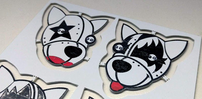
This method rewards planning. The designer begins with a simplified image, reduces it to a limited palette, then assigns each visual area to a PCB layer. In a board shaped like an animal, for instance, solder mask might define the body, exposed copper might form the eyes, white silkscreen might create fur texture, and LEDs might add interactive sparkle. Yes, it is basically graphic design with manufacturing constraints. No, the constraints do not make it less creative. They make it more interesting.
Layer-based PCB art works especially well for conference badges, decorative blinky boards, open-source hardware logos, and novelty electronics. It is affordable because it often uses standard fabrication options. It is also robust because the visual design is created by the same durable materials that make up the board itself.
Successful Experiment #2: Full-Color UV Printing
Full-color UV printing brings a different kind of freedom. Instead of relying only on solder mask, copper, and silkscreen, the manufacturer prints color artwork onto the PCB surface using UV-curable ink. This allows gradients, illustrations, icons, complex logos, and photographic-style graphics that would be difficult or impossible with standard silkscreen alone.
Successful UV-printed PCB projects usually start with a white solder mask background. White provides stronger color brightness and prevents the base board color from muddying the artwork. Designers often use this approach for front panels, decorative boards, educational kits, and display pieces. It is especially useful when the board is meant to be seen by customers, students, or fellow makers who appreciate a little visual seasoning with their electrons.
Still, UV printing is not magic confetti. Designers must account for alignment tolerance, ink durability, hole placement, component clearance, and the fact that soldering heat and flux residue can affect printed areas if the design is careless. The most successful boards keep high-detail artwork away from heavy soldering zones and leave breathing room around pads, connectors, switches, and mounting holes.
Successful Experiment #3: Multi-Color Silkscreen Services
Multi-color silkscreen services have made colorful boards more accessible to everyday makers. Instead of treating the silkscreen as a one-color legend, these workflows allow designers to import color artwork and output manufacturing files that preserve color information. Some services integrate this process through specific EDA tools, which can simplify ordering but may also require designers to adapt their workflow.
The appeal is obvious: a board can carry functional labels, branding, icons, and decorative graphics in multiple colors without requiring a separate sticker, label, or enclosure. For low-volume products, this can reduce assembly steps and create a more polished user experience. A sensor board with color-coded connectors is easier to use. A learning kit with colored zones feels friendlier. A badge with full-color character art becomes wearable hardware instead of just a rectangle with LEDs.
The best results come from designing artwork specifically for the PCB process. Large flat color areas, bold shapes, readable text, and clean contrast tend to reproduce better than tiny gradients and delicate details. If the design looks great only when zoomed to 800 percent on a monitor, it may not survive its trip through manufacturing with all its dignity intact.
Design Rules That Keep Colorful Boards Manufacturable
Great multicolor PCB design is equal parts creativity and discipline. Before sending a colorful board to production, designers should check the manufacturer’s capabilities for minimum trace width, solder mask clearance, silkscreen line width, text height, drill size, board outline tolerance, and layer registration. These numbers are not decorative suggestions. They are the difference between a crisp board and a tiny manufacturing tragedy.
Silkscreen should not overlap exposed pads. Solder mask openings should be large enough for reliable assembly but not so large that adjacent copper becomes vulnerable to solder bridging. Vias under artwork should be tented when possible to create a smoother surface. Components should not cover critical visual details unless that is part of the design. Mounting holes need clear space, especially when screws or standoffs will scrape the surface.
Color also affects inspection. White solder mask can show dirt and flux residue. Black solder mask can hide fine traces and make optical inspection harder. Matte finishes can reduce glare but may change the perceived brightness of printed artwork. ENIG looks beautiful but adds cost. These tradeoffs do not mean one option is “best.” They mean the right choice depends on whether the board is an engineering prototype, display piece, product faceplate, badge, or collectible.
Practical Examples of Multicolor PCB Success
One successful pattern is the artistic badge. Conference badges often use bold board shapes, plated edges, LEDs, capacitive buttons, and layered graphics. Multicolor design helps the badge become memorable before anyone even powers it on. Attendees wear it, photograph it, share it, and sometimes keep it for years. That is excellent marketing disguised as a circuit board.
Another strong example is educational hardware. A microcontroller learning board can use color-coded sections for power, inputs, outputs, communication, and sensors. Students can identify areas faster, wire modules with fewer mistakes, and understand the board layout more intuitively. In this case, color is not just pretty; it reduces friction.
Product branding is another natural use. A small synthesizer module, keyboard PCB, sensor hub, or development board can carry brand colors directly on the board. If the device has no enclosure or a transparent case, the PCB becomes part of the product’s visual identity. A clean multicolor board can make a small hardware startup look more established without adding expensive mechanical parts.
Common Mistakes in Multicolor Circuit Board Experiments
The first mistake is treating the PCB like paper. A board has holes, pads, copper, soldering heat, registration limits, and assembly equipment to consider. Fine art that ignores those constraints may arrive looking like it lost a bar fight with a drill press.
The second mistake is using low-contrast colors. A beautiful dark illustration on black solder mask may vanish under normal lighting. White text on pale yellow artwork may look clean on screen but become unreadable in real life. Always test contrast at actual board size.
The third mistake is forgetting components. Artwork placed under large connectors, displays, sockets, switches, or batteries may never be seen. Worse, it may interfere with assembly notes or polarity markings. In successful multicolor PCB design, the art supports the circuit instead of wrestling it for elbow room.
The fourth mistake is skipping prototypes. Even if the manufacturer provides a preview, the physical result can differ because ink, solder mask, copper finish, lighting, and scale all affect perception. A small prototype run is the safest way to confirm color, alignment, and durability before scaling up.
How to Plan a Multicolor PCB Project
Start with the purpose. Is the board supposed to teach, sell, impress, decorate, guide assembly, or become a collectible? That answer determines the design approach. A front panel may benefit from UV printing. A hacker badge may shine with exposed copper and LEDs. A production device may need modest color accents that improve usability without complicating manufacturing.
Next, choose the fabrication method. For simple art, use standard solder mask, copper, and silkscreen layers. For richer graphics, investigate multi-color silkscreen or UV printing. Then design at real scale. Print the artwork on paper at 100 percent size before ordering. If the text is too small on paper, it will not become magically readable on fiberglass. PCBs are useful, not enchanted.
Finally, prepare the files carefully. Keep a clean separation between electrical layers and artwork layers. Run design rule checks. Inspect Gerbers in an external viewer. Confirm that the board house supports your intended color process. If the service requires a specific tool or export method, follow it exactly. Creative freedom is wonderful, but the CAM department still needs files it can manufacture.
The Future of Multicolor Circuit Boards
Multicolor circuit boards are likely to become more common as digital printing, low-volume manufacturing, and design software continue improving. The line between PCB, product surface, and graphic interface is getting thinner. A board can be a circuit, label, dashboard, teaching diagram, decorative object, and brand statement all at once.
This does not mean every PCB needs to look like a festival poster. Many boards should remain simple, readable, and optimized for inspection. But for visible electronics, educational kits, maker projects, prototypes, collectibles, and premium small-batch devices, color is becoming a practical design tool. The best experiments prove that beauty and function are not enemies. They are roommates. Occasionally messy roommates, but roommates nonetheless.
Conclusion: Color Makes the Circuit Board Speak
Successful experiments in multicolor circuit boards show that PCB design is no longer limited to traces, pads, and component outlines. By using solder mask, silkscreen, copper, ENIG, UV printing, and multi-color workflows, designers can create boards that communicate clearly and look memorable. The strongest projects do not ignore engineering constraints; they use those constraints as part of the artwork.
Whether you are designing a conference badge, a product prototype, a front panel, or a learning board, color can improve usability and emotional appeal. It can tell users where to plug things in, make a brand feel more polished, and turn a simple circuit into an object people actually want to show off. In the world of hardware, that is a small miracle. Or at least a very attractive rectangle.
Additional Experiences From Real Multicolor PCB Experiments
One lesson from hands-on multicolor PCB projects is that the first version should be treated like a color proof, not a final masterpiece. Designers often discover that colors appearing vivid on a monitor become softer on white solder mask, darker on matte finishes, or slightly altered by the texture of the board. A good practical habit is to include a tiny color test strip on the edge of a prototype panel. Add sample blocks, line widths, text sizes, gradients, and small icons. When the boards arrive, that strip becomes a reference guide for the next revision. It is not glamorous, but neither is guessing.
Another experience is that bold design wins. Thin outlines, delicate shadows, and tiny decorative flourishes can look elegant in vector software, but PCBs reward confidence. Thick lines, clear color separation, generous spacing, and strong silhouettes usually survive fabrication better. When creating character art or logo art, simplify the illustration before exporting it. The goal is not to reproduce every microscopic detail; the goal is to make the board instantly recognizable at arm’s length.
Component placement also deserves special attention. In one common workflow, designers finish the electronic layout first, then place artwork around the functional areas. That works, but it can produce awkward results where the art feels trapped between connectors and mounting holes. A better method is to plan the mechanical outline, user-facing graphics, and major components together from the beginning. LEDs can become eyes. Buttons can become decorative dots. USB ports can align with graphic borders. Mounting holes can be integrated into the artwork instead of looking like someone attacked the design with a tiny hole punch.
For boards that will be assembled by hand, color can reduce mistakes. Use colored zones to separate voltage rails, signal groups, sensor areas, or connector types. Add clear polarity markers and keep them outside decorative clutter. A beautiful board that makes assembly confusing is not a success; it is a puzzle with solder fumes. The best multicolor experiments balance visual style with practical guidance.
Durability is another real-world issue. If the board will be handled often, mounted as a front panel, worn as a badge, or cleaned after soldering, avoid placing critical artwork where fingers, screws, flux, or tools will repeatedly touch it. Use keep-out areas around hardware. Consider whether the printed surface needs protection from abrasion. For display pieces, this may not matter much. For products, it matters a lot.
Finally, document the process. Save screenshots of settings, export steps, order options, color references, and photos of the finished board under normal lighting. Multicolor PCB production can involve special options, and future-you will not remember every checkbox. Future-you is busy and probably looking for coffee. Good notes make the second revision faster, cleaner, and more predictable. That is how experiments become repeatable success.
Note: This article synthesizes real PCB manufacturing practices, maker-community experiments, and current design guidance around solder mask, silkscreen, copper finish, UV printing, multi-color silkscreen workflows, and PCB art production without embedding source links.