Note: This article is written as copy-ready HTML for web publishing and is based on real digital logic concepts, educational computer architecture materials, and documented breadboard ALU projects.
There are easier ways to build an arithmetic logic unit. There are also faster ways, cheaper ways, cleaner ways, and ways that do not require turning your desk into a technicolor spaghetti farm of jumper wires. But few projects teach computer architecture as dramatically as building an 8-bit ALU entirely from NAND gates. It is the electronics equivalent of baking a wedding cake using only a toaster: technically possible, oddly beautiful, and guaranteed to make you respect every modern microprocessor a little more.
An ALU, or arithmetic logic unit, is the part of a processor that performs operations such as addition, subtraction, bitwise logic, comparisons, and sometimes shifts. In a modern CPU, the ALU is buried inside silicon, surrounded by registers, control logic, caches, pipelines, prediction units, and other wizardry. In a breadboard project, the same idea becomes gloriously visible. You can watch binary numbers arrive, carries ripple from one bit to the next, LEDs blink with the smug confidence of correct math, and one loose wire destroy your afternoon.
The reason this project is so fascinating is simple: the NAND gate is universal. With only NAND gates, you can construct NOT, AND, OR, XOR, multiplexers, adders, and eventually a full ALU. That means an 8-bit NAND-only ALU is not merely a stunt. It is a hands-on proof that the complicated machinery of computation can emerge from one tiny logical building block repeated many, many, many times. Somewhere in there is a life lesson. Possibly also a warning about buying jumper wires in bulk.
What Is an 8-Bit ALU?
An 8-bit ALU processes two 8-bit binary inputs. Each input can represent values from 0 to 255 if interpreted as unsigned numbers, or from -128 to 127 if interpreted using two’s complement signed arithmetic. The ALU accepts control signals that tell it what operation to perform, then produces an 8-bit result along with status outputs such as carry, zero, overflow, or negative flags depending on the design.
In a simple educational computer, the ALU might handle only addition and subtraction. In a more flexible design, it may also perform AND, OR, XOR, NOT, increment, decrement, pass-through, and comparison operations. The core idea remains the same: the ALU is the processor’s workbench. Data comes in, the selected operation happens, and the result goes back to a register, bus, memory path, or output display.
Why 8 Bits Still Matter
Eight-bit computing is not just nostalgia wearing a pocket protector. The 8-bit word size is small enough for humans to understand and large enough to demonstrate real CPU behavior. With 8 bits, you can show carry propagation, binary overflow, two’s complement subtraction, bus timing, instruction control, and register transfers without needing a microscope or a therapy session.
That is why 8-bit breadboard computers remain popular in maker education. They reveal the hidden logic inside computers in a way that software simulations cannot fully replace. A simulator can show a signal changing from 0 to 1. A breadboard ALU lets you see the LED change, hear the relay-like click of your own brain understanding it, and occasionally smell the faint aroma of a chip inserted backward. Education has texture.
Why Build an ALU Entirely From NAND Gates?
At first glance, building an ALU from only NAND gates sounds deliberately inconvenient. After all, standard integrated circuits already exist for adders, multiplexers, buffers, and logic functions. A practical designer normally chooses the right chip for the job. But a NAND-only design is not about convenience. It is about fundamentals.
The NAND gate produces a low output only when all its inputs are high. In every other input combination, its output is high. This simple behavior gives it a superpower: NAND can be combined to create every other Boolean logic function. Tie the two inputs together and you get NOT. Use NAND followed by NAND-as-inverter and you get AND. Combine NAND structures differently and you get OR through De Morgan’s laws. Build more layers and you get XOR, adders, selectors, and full arithmetic circuits.
That universality makes NAND the perfect educational building block. It strips digital electronics down to one rule and asks, “How far can we go?” The answer is: surprisingly far. Far enough to build an 8-bit ALU. Far enough to build a processor. Far enough, in theory, to build a complete computer from first principles.
The Building Blocks: From NAND to Arithmetic
A NAND-only ALU does not appear fully formed like a silicon unicorn. It is assembled from smaller logic structures. Each layer builds meaning from the layer below it.
NOT, AND, and OR From NAND
The simplest transformation is the inverter. Connect both inputs of a NAND gate to the same signal, and the output becomes the opposite of that signal. If A is 1, NAND(A,A) is 0. If A is 0, NAND(A,A) is 1. Congratulations: one NAND gate just became a NOT gate.
To create AND, take A NAND B and invert the result with another NAND gate. Since NAND is “not AND,” inverting it gives plain AND. OR can be created by first inverting both inputs and then feeding those inverted signals into a NAND gate. This works because of De Morgan’s law: A OR B equals NOT(NOT A AND NOT B). The NAND gate is doing more gymnastics than a caffeinated logic professor, but the result is clean.
XOR: The Dramatic One
XOR, or exclusive OR, is essential for binary addition because the sum bit of a half adder is A XOR B. XOR outputs 1 when its inputs differ and 0 when they are the same. It takes more NAND gates than basic logic functions, which is one reason arithmetic circuits grow quickly when built from a single gate type.
A common NAND-only XOR uses four NAND gates. First, NAND the two inputs. Then NAND each original input with that intermediate result. Finally, NAND those two outputs together. The result behaves exactly like XOR. It is elegant, slightly sneaky, and a reminder that digital design is often about rearranging truth tables until they agree to cooperate.
Half Adders and Full Adders
A half adder adds two one-bit values. It has two outputs: sum and carry. The sum is produced by XOR. The carry is produced by AND. A full adder goes one step further by accepting a carry-in bit from the previous stage. This is what allows multiple one-bit adders to be chained into a multi-bit adder.
For an 8-bit ALU, eight full adders are usually connected in a row. Bit 0 adds the least significant bits and produces a carry. That carry goes into bit 1, which may produce another carry, and so on until bit 7. This structure is called a ripple-carry adder because the carry signal ripples through the chain. It is easy to understand and build, though not the fastest approach because the final result must wait for carry propagation.
How an 8-Bit NAND-Only ALU Performs Addition
Addition is the heart of many ALU designs. Once addition works, subtraction can often be implemented with clever input manipulation, and comparisons can be derived from subtraction results. In a NAND-only design, each full adder is built from NAND-based XOR, AND, and OR equivalents.
Imagine adding two 8-bit numbers: A and B. Each bit position has one bit from A, one bit from B, and one carry-in. The full adder produces a sum bit and a carry-out. After all eight stages operate, the ALU has an 8-bit result and possibly a carry-out from the most significant bit.
For example, adding 00000101 and 00000011 should produce 00001000. In decimal, that is 5 + 3 = 8. On a breadboard ALU, each result bit might be connected to an LED. When the operation is correct, the fourth LED from the right lights up and the others stay dark. It is a tiny fireworks show for binary arithmetic.
Subtraction With Two’s Complement
Subtraction is often handled using two’s complement arithmetic. Instead of designing a completely separate subtractor, the ALU can invert the B input and add 1. In binary, A – B can be performed as A + NOT(B) + 1. That extra 1 is usually introduced through the carry-in of the least significant full adder when subtraction mode is selected.
This is where NAND gates become particularly useful. Since inverters can be made from NAND gates, the B input can be conditionally inverted. A control signal selects whether the ALU should use B directly for addition or inverted B for subtraction. The same control signal can also provide the initial carry-in. If the subtract signal is 0, the ALU adds. If it is 1, the ALU performs two’s complement subtraction.
For example, 00001000 minus 00000011 becomes 8 – 3. The ALU inverts 3, adds 1, and combines it with 8. The final result is 00000101, or 5. The circuit does not “know” subtraction as a human concept. It simply follows logic rules. This is both humbling and mildly insulting, because the breadboard is doing math by being stubbornly literal.
Logic Operations: AND, OR, XOR, and Beyond
An ALU is not only an arithmetic unit. It is also a logic unit. Bitwise operations are essential for masking, testing, toggling, clearing, and manipulating data. In an 8-bit ALU, a bitwise AND compares each pair of input bits independently. Bit 0 of A is ANDed with bit 0 of B, bit 1 with bit 1, and so on.
Bitwise OR is useful for setting bits. XOR is useful for toggling bits or comparing differences. NOT can invert an input. More elaborate ALUs may include pass-through functions, zero output, increment, decrement, or comparison signals such as equal and less-than. All of these can be made from NAND gates, although each added function increases gate count, wiring complexity, and the chance that one jumper wire is quietly plotting against you.
Control Signals and Multiplexers
An ALU needs a way to choose which operation appears at the output. If the circuit computes addition, AND, OR, and XOR at the same time, it still needs selection logic to decide which result is forwarded. This is where multiplexers enter the story.
A multiplexer, or mux, selects one of several inputs based on control signals. Like everything else in a NAND-only ALU, a mux can be built from NAND gates. A simple two-input mux can choose between input A and input B using a select line. Larger multiplexers can be built by combining smaller ones.
In a practical 8-bit design, each bit of the output may require its own mux path. That means the selection logic is repeated eight times. This repetition is why breadboard ALUs look so dramatic. The logic itself is simple, but simple logic multiplied across eight bits becomes a small city of chips, wires, and labels.
Status Flags: The ALU’s Little Report Cards
Many ALUs produce status flags. These are single-bit signals that describe the result. A zero flag indicates that the output is 00000000. A carry flag indicates that addition produced a carry out of the most significant bit. A negative flag usually reflects the most significant bit in signed two’s complement arithmetic. An overflow flag indicates that signed arithmetic produced a result outside the representable range.
Flags are important because control logic can use them for branching. A processor can compare two numbers by subtracting them and checking whether the result is zero, negative, or overflowed. Without flags, a CPU would be very bad at decisions, which would make it less of a computer and more of a very expensive blinking ornament.
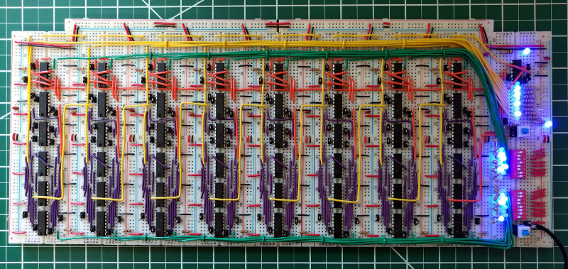
The Physical Challenge: Breadboards, CMOS Chips, and Wiring Chaos
The conceptual design of a NAND-only ALU is tidy. The physical version is where humility arrives wearing safety goggles. A typical NAND-only implementation may use many quad NAND gate ICs, such as 4011-family CMOS chips. Each package contains four two-input NAND gates, so the number of chips rises quickly as the ALU grows.
Eight full adders alone require a significant number of NAND gates. Add subtraction control, output selection, logic functions, flags, LEDs, switches, and bus connections, and the project can easily spread across multiple breadboards. Power distribution becomes important. Signal naming becomes essential. Wire color discipline becomes the difference between debugging and archaeology.
Propagation delay also matters. Each gate takes a small amount of time to respond after its inputs change. In a ripple-carry adder, the carry must travel through multiple stages. At human-operated breadboard speeds, this is usually acceptable. At high clock speeds, it becomes a limitation. This is why real processors use faster adder structures, optimized layouts, and transistor-level design techniques. The breadboard ALU is not trying to beat a modern CPU. It is trying to explain one.
Why NAND-Only Design Is a Great Learning Tool
Building an 8-bit ALU from NAND gates forces you to understand digital electronics at the level where abstractions become physical. You cannot hide behind a plus sign. You must ask what addition means in gates. You cannot wave at “logic” as a vague concept. You must route it from pin to pin.
This project teaches Boolean algebra, modular design, binary arithmetic, bus architecture, debugging strategy, timing, and documentation. It also teaches patience, which is not usually listed in computer architecture textbooks but should probably be chapter one.
The best part is that the project scales intellectually. Beginners can start by building a NAND inverter, then an XOR, then a half adder. Intermediate builders can chain full adders into a 4-bit or 8-bit ripple-carry adder. Advanced builders can add operation selection, flags, tri-state bus behavior, instruction decoding, and eventually a whole CPU.
Specific Example: Adding and Subtracting on an 8-Bit NAND ALU
Suppose the A input is 00001100 and the B input is 00000101. In decimal, these are 12 and 5. In addition mode, the ALU feeds B directly into the full adder chain and sets the initial carry-in to 0. The result becomes 00010001, or 17.
In subtraction mode, the ALU inverts B and sets the initial carry-in to 1. So instead of adding 5, it adds the two’s complement form of -5. The result becomes 00000111, or 7. The same adder hardware performs both operations. The only difference is how the B input and carry-in are controlled.
This is one of the most satisfying moments in digital logic. A circuit that seemed built for addition suddenly handles subtraction without needing a separate subtractor. It feels like cheating, but it is really mathematics being economical.
Common Mistakes When Building a NAND-Only ALU
The first common mistake is underestimating wiring. A schematic may look neat on screen, but breadboards impose physical constraints. Pins are not always where you wish they were. Jumpers cross. Power rails split. Ground connections hide in plain sight. Label everything early, or future-you will have opinions about past-you.
The second mistake is testing too much at once. Do not build the entire ALU and then ask why it does not work. Test each NAND gate chip. Test each derived gate. Test each XOR. Test each full adder. Then test a 2-bit chain before expanding to 8 bits. Debugging is much easier when the suspect list is short.
The third mistake is ignoring power stability. CMOS logic inputs should not float. Unconnected inputs can behave unpredictably, picking up noise and turning your beautiful ALU into a random number generator with artistic ambitions. Use proper pull-up or pull-down resistors where needed, keep power rails consistent, and decouple ICs when appropriate.
How This Project Connects to Modern Computing
A NAND-only 8-bit ALU may look primitive compared with a modern processor, but the underlying principles still matter. Modern CPUs use billions of transistors, but those transistors still implement logic. The layers are more complex, the scale is microscopic, and the speed is astonishing, yet the foundation remains Boolean computation.
Learning NAND-only design is like learning grammar before writing novels. You may not diagram every sentence later, but understanding structure makes you better at the craft. Likewise, once you understand how NAND gates can become adders and ALUs, higher-level topics such as instruction sets, pipelining, microcode, and hardware description languages become less mysterious.
Experiences and Practical Lessons From Building an 8-Bit ALU Entirely From NAND Gates
The most memorable experience related to building an 8-bit ALU entirely from NAND gates is the moment when theory stops being polite. On paper, the circuit is clean: eight slices, each slice containing a full adder, control signals, optional inversion, and output logic. On the breadboard, the circuit becomes a neighborhood. Every signal needs a road. Every road needs to avoid traffic. Every chip needs power and ground. Suddenly, “just use NAND gates” sounds less like a design philosophy and more like a dare issued by someone who has never paid for jumper wires.
One useful lesson is to build the ALU as repeated bit-slices. Instead of thinking about all 8 bits at once, design one complete 1-bit section and verify it thoroughly. That section should accept A, B, carry-in, and mode control signals, then produce sum, logic output, and carry-out as needed. Once one slice works, replicate it seven more times. This modular approach makes the project manageable and mirrors how many real hardware systems are designed.
Another important experience is discovering that visual organization is not cosmetic. Color-coded wires can save hours. For example, red and black should be reserved for power and ground. One color can represent A inputs, another B inputs, another carry signals, and another control lines. The exact color scheme matters less than consistency. When a circuit has hundreds of connections, neat wiring is not vanity. It is survival.
Testing should feel almost boring. That is a good thing. Start by testing NAND-as-NOT. Then test NAND-based AND and OR. Then test XOR. Then test a half adder, a full adder, and finally a chain of two full adders. Only after those pieces behave should the full 8-bit structure come together. A rushed build often creates multiple simultaneous bugs, and multiple simultaneous bugs are where optimism goes to retire.
One surprisingly practical tip is to keep a written test table. For a full adder, test all eight combinations of A, B, and carry-in. For an 8-bit adder, test simple cases first: 0 + 0, 1 + 1, 15 + 1, 127 + 1, 255 + 1. For subtraction, test 8 – 3, 5 – 5, 0 – 1, and 128 – 1. These cases reveal carry behavior, zero detection, signed overflow, and bit propagation errors. LEDs are helpful, but a written checklist keeps you honest.
The emotional arc of the project is also real. At first, you feel powerful because NAND gates can do anything. Then you feel betrayed because “anything” requires many gates. Then you feel clever again when the first addition works. Finally, you feel suspicious, because every correct output seems too good to trust. That suspicion is healthy. Hardware rewards careful verification.
The biggest takeaway is that a NAND-only ALU turns abstraction into craftsmanship. It teaches that computers are not magic boxes. They are organized consequences. A 1 becomes another 1 because a gate says so. A carry moves because the previous stage produced it. A subtraction works because two’s complement arithmetic makes it possible. Once you see those facts blinking on a breadboard, software feels different. Every line of code eventually depends on tiny logical decisions happening at ridiculous speed.
Conclusion
An 8-bit ALU entirely from NAND gates is not the easiest way to build arithmetic hardware, but it is one of the clearest ways to understand it. The project demonstrates the universality of NAND logic, the structure of full adders, the elegance of two’s complement subtraction, and the practical realities of physical digital design. It also proves that complexity does not always begin with complex parts. Sometimes it begins with one simple gate repeated with discipline, patience, and a heroic amount of wire.
For students, hobbyists, and anyone curious about computer architecture, a NAND-only ALU is a brilliant bridge between theory and hardware. It shows how binary numbers move, how decisions are selected, how status flags guide control logic, and how a processor’s mathematical heart can be built from the humblest possible component. Modern computers may hide their logic inside microscopic silicon, but the principles remain visible on a breadboard. And yes, the wiring may look terrifying. That is part of the charm.