There comes a magical moment in almost every electronics project when the circuit works, the LEDs blink, the firmware behaves, and then reality shows up wearing steel-toe boots and asks, “Cool. So where’s the case?” That is exactly where PCB casing and PCB instrument panels stop sounding like a weird maker stunt and start looking like a smart design move.
Using a printed circuit board as a casing or front panel is not just a visual gimmick. It is a practical shortcut that blends mechanical structure, labeling, mounting, and aesthetics into one manufacturable part. Instead of designing a separate faceplate, printing labels, drilling plastic, and hoping everything lines up like a miracle, you can turn the PCB itself into the enclosure wall, control panel, or even the whole box. In the best cases, it looks clean, professional, and delightfully overqualified for the job.
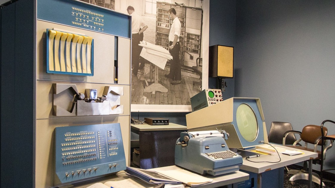
Recent maker projects have pushed this idea further, including retro-computing replicas and custom control surfaces built from multiple PCB panels soldered or fastened together. But the underlying concept is older and simpler: FR-4 is strong, dimensionally stable, easy to fabricate accurately, and already speaks fluent holes, slots, cutouts, graphics, and mounting points. In other words, it is not just the thing that holds the electronics. Sometimes it is the product’s skin.
Why Use a PCB for a Casing or Instrument Panel?
The biggest advantage is precision. A standard enclosure often forces you into a long romance with calipers, drills, files, and regret. A PCB front panel, by contrast, comes back from fabrication with connector openings, switch holes, LED windows, mounting holes, and printed labels already aligned. That makes a PCB front panel especially attractive for test instruments, synth modules, bench controllers, retro replicas, and low-volume products where custom sheet metal or molded plastic would be expensive overkill.
Another advantage is graphics. A PCB gives you access to silkscreen, solder mask color, exposed copper, plated holes, and even carefully planned translucent or backlit areas. You are not adding a sticker after the fact and pretending it is industrial design. You are building the visual identity into the board itself. For instrument panels, that is a huge win. Labels stay crisp, legends line up properly, and the result looks less “science fair” and more “small-batch hardware startup that drinks decent coffee.”
There is also a workflow advantage. Modern PCB tools and ECAD-MCAD workflows make it easier to think about the board as a mechanical object, not just a nest of traces. That means your custom electronics enclosure can be modeled around connector height, button travel, display openings, board supports, and clearances before you ever order fabrication. Translation: fewer surprise collisions, fewer “why is the USB port half-buried in the wall?” moments, and fewer opportunities to invent new curse words.
What Makes PCB Material So Useful Structurally?
Rigid PCBs are commonly built on fiberglass-reinforced epoxy, usually FR-4. That gives them a combination of stiffness, machinability, and dimensional predictability that works surprisingly well for panels and light structural parts. A PCB is not a steel chassis, of course, but for a control panel, side wall, bracket, light-duty box, or decorative structural shell, it punches above its weight.
Thickness matters. A thin board may look sleek, but it can flex too easily if it is doing real structural work. A thicker board is better when the panel holds switches, connectors, or knobs that users will press, twist, and occasionally bully. If the board is just a faceplate or a cosmetic skin, moderate thickness may be enough. If it is the actual casing wall, you need to think like a mechanical designer: stiffness, edge support, fastening strategy, and how much force the user is likely to apply.
The board’s finish matters too. Solder mask color changes the whole personality of a panel. Matte black can look serious and premium. White can feel clean and technical. Exposed copper or gold-colored finish can create elegant labels, trim, or indicator markings. Suddenly your circuit board is no longer hiding in shame behind a plastic shell. It is out front, dressed for the occasion.
How PCB Casing Design Actually Works
1. Treat the board outline like a mechanical drawing
When you use a PCB as a panel or enclosure part, the board outline is everything. Edge cuts, slots, cutouts, radii, mounting holes, and hole tolerances all become critical. This is where many first-time designers make a classic mistake: they spend hours polishing trace routing and then draw the enclosure features like they are doodling on a napkin.
Do not do that. The PCB mechanical design needs to define where switches, connectors, standoffs, displays, screws, and supports live. If the panel mates to another case part, the hole pattern and datum strategy need to be deliberate. If there is a rotary encoder near the edge, the nut clearance matters. If a USB connector pokes through a slot, the shell dimensions matter. A beautiful board that misses the opening by one millimeter is still a beautiful board you cannot use.
2. Use cutouts and slots intelligently
PCB fabricators can produce plated and non-plated slots, internal cutouts, and routed contours, but these features must be called out correctly in manufacturing files. This matters for instrument panels because rectangular connector openings, switch windows, fuse access, and display apertures often need something more refined than round holes. When used properly, these features let a PCB panel replace laser-cut acrylic, machined sheet stock, or hand-modified plastic.
The golden rule is simple: design the opening for the real hardware, not the imaginary version of it living in your optimism. Measure the connector body, bezel, nut diameter, keying features, and insertion path. Then leave sensible tolerance. Electronics love precision; assembly loves forgiveness. Both deserve a seat at the table.
3. Build the graphics into the board
This is where PCB instrument panels become really fun. Silkscreen can label controls, indicate polarity, show scales, and add branding. Solder mask can define visual fields or contrast zones. Exposed copper can create decorative accents or conductive touch areas. Some builders even remove copper and mask in selected regions to create backlit text or indicator windows. It is basically graphic design with the added thrill of drill charts.
For panels with knobs or analog-style scales, use silkscreen for tick marks and numerals, but keep readability in mind. Tiny legends may look elegant on screen and then vanish in real life unless the user happens to be an eagle. Contrast, line thickness, and spacing matter. A great instrument panel is not just pretty. It is readable under actual room light by actual humans.
4. Choose a joining method before you get clever
A full printed circuit board enclosure usually involves multiple panels joined together. There are several ways to do that: screws into standoffs, spacers and corner brackets, interlocking tabs, edge soldering, or hybrid methods. Edge soldering is especially appealing for maker builds because it can produce strong, tidy seams with very little extra hardware. But it also demands planning. The edge geometry, copper placement, assembly access, and soldering sequence all need thought up front.
If you want something serviceable, screws are your friend. If you want something rigid and almost monolithic, soldered seams may be better. If you want something fast and experimental, even temporary scaffolding and tack assembly can help during prototyping. The point is to choose the method early, because your hole pattern, edge design, and panel layout all depend on it.
Best Use Cases for PCB Panels and Cases
PCB-based front panels shine when you need low to medium production volume, precise labeling, and a custom shape. A few standout examples include bench instruments, audio gear, modular synth modules, programmer/debugger boxes, scientific controls, educational kits, and retro-computing replicas. In these projects, the panel does not just cover the electronics. It communicates how the device is used.
PCB casings also make sense for compact devices where every millimeter counts. Exposed pads can replace bulky programming headers. Connector placement can be optimized around the case geometry. Mounting holes and supports can be integrated into the same design file. That makes the board and enclosure feel like one system instead of two departments barely speaking to each other.
And yes, there is an undeniable style factor. A PCB enclosure has a distinct look that can feel futuristic, retro-industrial, or wonderfully nerdy depending on the finish and graphics. In the right product category, that is not a compromise. That is branding.
Where PCB Casing Falls Short
Let’s not pretend PCB enclosures solve every problem. They do not. If your product needs strong environmental sealing, serious impact resistance, soft-touch ergonomics, or consumer-grade drop tolerance, a traditional enclosure material may be a better fit. Plastic and metal still win plenty of arguments.
Thermal performance is another concern. Compact electronics already struggle with heat, and turning the board into part of the enclosure can complicate airflow and thermal paths. You need to think about hot components, venting, copper distribution, clearances, and whether the casing is trapping warmth around the parts most likely to complain first. Electronics do not enjoy saunas nearly as much as humans do.
Then there is ruggedness. If the device will face vibration, moisture, shock, harsh handling, or outdoor use, the enclosure strategy must reflect that. A PCB wall can be precise and attractive while still being vulnerable if the assembly lacks proper supports, sealing, or strain relief. Connectors especially need attention. They are often where mechanical reality and electrical ambition collide.
Design Tips for Better PCB Instrument Panels
Make the panel readable from day one
Use clear typography, consistent symbol language, and enough contrast between labels and the mask color. Separate user-facing markings from assembly references. The operator does not need to see every designator unless your ideal user is a repair technician wearing a headlamp.
Model connector height and body shape
3D checks matter. The board may fit in outline view and still fail in real life because the connector shell, display frame, or switch body collides with another panel. Use 3D CAD or board visualization tools early. It is much cheaper to discover a collision on-screen than after the courier arrives.
Leave room for fingers, tools, and tolerances
A perfect CAD model can still become an annoying product if a user cannot tighten a nut, reach a button, or plug in a cable without scraping adjacent hardware. Allow sane spacing around ports and controls. The world contains hands, not just dimensions.
Think about manufacturing files as communication
Gerbers, drill files, fab drawings, border definitions, and notes for slots or non-plated holes all help the board house understand what you actually want. A PCB panel is part graphics job, part mechanical job, part electrical design, and part “please do not interpret my silence creatively.” Clear manufacturing data reduces unpleasant surprises.
A Smart Example of the Idea in Action
A great example of this trend is the growing number of maker builds that use PCB panels for retro-style control systems and replica machines. The appeal is obvious. Old-school instruments and computing interfaces often rely on dense arrangements of switches, lights, legends, and apertures. A PCB is naturally good at all of those. It can carry LEDs, define exact switch spacing, print the labels, and form the visible control surface all at once.
That makes PCB instrument panels especially compelling in projects where appearance and authenticity matter as much as the electronics. Instead of building a faceplate first and then forcing the circuit to match it, the PCB lets the visual and electrical design evolve together. That is not just efficient. It is elegant.
Conclusion
Hacking a printed circuit board to create casing and instrument panels is one of those ideas that sounds like a shortcut until you realize it is actually a design philosophy. It treats the PCB as more than a hidden carrier of parts. It becomes structure, interface, branding, and documentation in one object.
Done well, a PCB enclosure can reduce assembly steps, improve alignment, simplify labeling, and create a distinctive visual identity. Done badly, it can become an expensive rectangle of regrets with a USB port trapped behind fiberglass. The difference is thoughtful mechanical planning, solid manufacturing communication, and respect for real-world use.
For prototypes, small-batch products, test gear, retro replicas, and custom control panels, this approach is incredibly compelling. It turns the board into the box and the interface into the fabrication file. And honestly, that is pretty cool. Nerdy? Absolutely. Effective? Also absolutely. Sometimes the best enclosure for your electronics is the one your electronics were already made from.
Common Real-World Experiences When Building PCB Cases and Panels
One of the most common experiences builders report is that the first PCB panel feels almost too easy. You send out the file, get back a beautiful board with crisp legends, perfect holes, and a finish that makes your project look far more professional than it has any right to. Then assembly begins, and you discover the classic gap between “it fits in CAD” and “it fits while a human is holding a screwdriver.” That is usually the moment when people become lifelong believers in tolerance, spacing, and mockups.
Another recurring lesson is how surprisingly satisfying PCB graphics can be. When the silkscreen is clean, the solder mask color is chosen well, and the panel layout is balanced, the result can look fantastic straight out of the box. Builders often say the panel feels like the first moment the project becomes a real product instead of a lab experiment. Even simple additions like icons, alignment marks, or properly spaced legends can make a device feel polished and intuitive.
There is also the experience of learning how mechanical forces travel through a design. A toggle switch on a PCB front panel is not just an electrical component. It is also a lever that invites fingers to apply force over and over again. A USB cable does not merely carry data; it yanks sideways on the connector when someone plugs it in carelessly. A rotary encoder nut can save a panel or slowly chew through your confidence. After one or two builds, designers start placing supports, screws, brackets, and reinforced areas much more thoughtfully.
Many builders also discover that PCB-based enclosures reward iteration. The first version proves the concept. The second version fixes spacing and improves the labels. The third version starts showing off a little with cleaner graphics, better seams, nicer cutouts, maybe even a backlit legend or exposed-copper accent. Because board fabrication is accessible, the design can mature quickly. That fast feedback loop is a huge part of the appeal.
Perhaps the most interesting experience is psychological: once someone builds one successful PCB panel, they start seeing opportunities everywhere. A test fixture could use one. A synth controller could use one. A small lab instrument could absolutely use one. Before long, the designer is looking at ordinary plastic enclosures the way a chef looks at plain toast: fine, technically edible, but not exactly exciting. That may be the real hack here. PCB casings and instrument panels do not just solve a packaging problem. They change the way you think about the relationship between electronics, mechanics, and product design.