Note: This article discusses home PCB through-plating at a high level for educational and editorial purposes. Any real work involving PCB chemicals, drilling dust, plating baths, etchants, or soldering should follow safety data sheets, local hazardous-waste rules, proper ventilation, and experienced supervision. The magic smoke is funny only when it stays inside the components.
Introduction: When Your PCB Fab Is Too Far Away
For years, hobbyists have accepted a simple bargain: design a board, export Gerbers, upload files to a PCB manufacturer, and wait. The results are usually excellent, inexpensive, and far cleaner than turning a garage into a tiny copper-themed science fair. But waiting is still waiting. When a project is stuck because one trace needs to hop from the top layer to the bottom layer, even a budget board house on the other side of the world can feel as distant as Mars.
That is why the phrase “two-layer PCBs with through-plating at home” gets electronics makers to sit up a little straighter. A single-sided etched PCB is useful. A double-sided PCB with hand-soldered wire jumpers is better. But a true two-layer PCB with plated-through vias? That is the difference between “I made a board” and “I appear to have accidentally opened a micro-fabrication department next to the laundry detergent.”
The open-source approach often discussed under the name Process 01 showed that the impossible-looking part of DIY PCB fabricationmaking reliable copper connections through drilled holescan be approached at home with documented, repeatable, community-reviewable methods. It does not make the process effortless. It does not make chemistry optional. And it definitely does not mean every kitchen should become a board shop. But it does prove something important: the knowledge barrier is shrinking.
What Makes Two-Layer PCBs So Useful?
A printed circuit board is more than a flat piece of fiberglass with shiny lines. It is the physical map of an electrical idea. On a single-sided PCB, every signal must travel on one copper layer. That sounds manageable until one trace needs to cross another. Then the designer must reroute, add jumpers, use awkward component placement, or whisper motivational quotes at KiCad at 2 a.m.
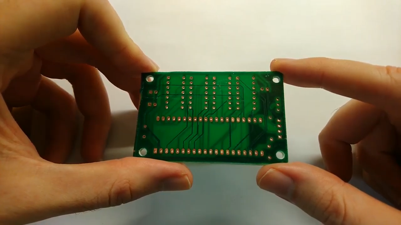
A two-layer PCB solves much of that pain by placing copper on both sides of the board. Signals can travel on the top layer, the bottom layer, or both. Power and ground routing becomes cleaner. Components can be arranged more logically. Compact designs become realistic instead of looking like a plate of copper spaghetti.
The Role of Vias
The hero of the two-layer board is the via. A via is a small drilled hole that creates an electrical connection between layers. In commercial boards, the inside wall of the hole is coated with copper, forming a vertical conductive barrel. That barrel links the top copper pad to the bottom copper pad. The result is called a plated-through hole, or PTH.
Without plated-through vias, a DIY two-layer board still works, but every layer change needs help. Makers commonly use small bits of wire soldered on both sides, eyelets, rivets, or component leads. These tricks can be perfectly fine for prototypes, but they add labor, height, resistance, reliability concerns, and many opportunities to say words not approved for polite datasheets.
Why Through-Plating at Home Has Been So Difficult
At first glance, through-plating sounds easy: drill a hole, put copper inside it, done. Unfortunately, the wall of a drilled PCB hole is mostly fiberglass and epoxy, which are not conductive. Copper will not electroplate onto an insulating surface unless that surface is first prepared to accept it.
Commercial PCB fabrication handles this with controlled drilling, cleaning, desmearing, chemical activation, electroless copper deposition, electroplating, imaging, etching, solder mask, and testing. The process is industrial for good reasons. It must produce thousands of holes that work electrically and mechanically, even after soldering heat, vibration, humidity, and years of use.
In a home workshop, the challenge is not simply “can copper be deposited?” The better question is: can copper be deposited evenly enough inside small holes, with enough adhesion, without destroying the board, poisoning the sink, or turning the bench into a museum exhibit titled Bad Choices in Brown Stains?
The Open-Source Breakthrough: Process, Not Mystery
The exciting part of the open-source method is not that it invented plated holes from scratch. PCB manufacturers have used plated-through holes for decades. The breakthrough is that the method translates a professional idea into a documented, learnable, maker-scale process. It invites testing, criticism, improvement, and adaptation.
At a high level, the method begins with a drilled double-sided copper-clad board. The hole walls must be made capable of accepting copper. This is generally done through a surface-activation stage, followed by a thin chemical copper deposition stage. That thin conductive layer acts like a seed. After that, electroplating can thicken the copper so the via becomes useful rather than merely decorative.
Once the holes are plated, the board can be patterned, etched, cleaned, protected, and assembled. In other words, the process tries to bring the missing industrial stepreliable vertical copper connectionsinto the home-lab workflow.
Why “Open Source” Matters Here
Open source is not just a software license wearing a hoodie. In hardware, open documentation changes the entire learning curve. Instead of relying on vague forum posts, half-remembered recipes, or “trust me bro” chemistry, makers can examine the logic of the process, compare results, publish failures, and improve the method.
That matters because home PCB fabrication has many variables: drill quality, board material, hole size, cleaning, solution condition, agitation, temperature, exposure alignment, plating time, current density, and storage. A closed recipe can fail mysteriously. An open process can be debugged like a circuit.
How This Compares With Common DIY PCB Methods
Single-Sided Etching
Single-sided etching is the classic gateway into homemade PCBs. It is simple in concept: protect the copper you want to keep, remove the rest, drill holes, solder parts. It is great for simple circuits, audio projects, LED boards, sensor breakouts, and learning. But once routing gets dense, single-sided boards become frustrating.
Double-Sided Boards With Wire Vias
Many hobbyists already make double-sided boards by aligning artwork on both sides and then soldering bits of wire through via holes. This method is practical and surprisingly effective. For one or two prototypes, it may still be the fastest path. But if a design has dozens of vias, the hand-soldered approach starts feeling like sewing chainmail for a very tiny knight.
CNC-Milled PCBs
CNC PCB milling removes unwanted copper mechanically instead of chemically. It is clean in some ways and fast for certain jobs. However, tiny isolation gaps, tool wear, board flatness, and through-hole interconnects remain challenges. Milling can make excellent single-sided and some double-sided prototypes, but plated-through vias are still a separate problem.
Professional PCB Fabrication
Commercial fabrication remains the best choice for polished, repeatable, production-ready boards. It offers solder mask, silkscreen, controlled tolerances, surface finishes, electrical testing, and multilayer options. The open-source home method does not replace fab houses. It fills a different niche: rapid learning, urgent prototypes, process experimentation, and maker independence.
Design Rules for Home Through-Plated Boards
Designing for homemade through-plating should be more conservative than designing for a professional PCB service. A fab house may tolerate small drills, narrow annular rings, tight spacing, and dense packages. A home process deserves room to breathe. Copper, like people, behaves better when not forced into stressful corners.
Use Larger Vias Than You Think You Need
Small vias look elegant in CAD, but they are harder to drill accurately and harder to plate reliably. Larger holes provide more surface area, better cleaning access, and more tolerance for alignment errors. For home boards, generous via dimensions are not a sign of weakness; they are a sign that the designer has met a drill press before.
Give Annular Rings Extra Space
The annular ring is the copper donut around a drilled hole. If the drill wanders or alignment shifts, a narrow ring can break, leaving a weak or open connection. Professional design rules often specify minimum annular rings, but home fabrication should go larger. Bigger pads may look less sleek, yet they dramatically improve survivability.
Avoid Dense Fine-Pitch Routing
Home through-plating is best suited to boards that are clever, not microscopic. Microcontroller boards, audio circuits, simple power supplies, keyboard controllers, sensor boards, and educational prototypes are realistic. High-speed RF boards, dense BGAs, impedance-controlled USB-C layouts, or tiny wearable modules are better left to professional fabs unless your workshop also contains a cleanroom and a suspiciously serious lab coat.
Add Test Coupons
A smart layout includes test features. Add a few spare vias, daisy chains, or resistance-check structures near the board edge. These sacrificial features help verify plating quality before trusting the actual circuit. Testing a via chain is much nicer than discovering a hidden open circuit after the last component is soldered and the project enclosure is already closed.
Where KiCad and Open Tools Fit In
The home PCB revolution is not only about chemistry. It is also about tools. Open-source EDA software such as KiCad gives makers professional-style schematic capture, PCB layout, design-rule checking, Gerber output, drill-file generation, 3D viewing, and inspection tools without locking the knowledge behind expensive software.
For homemade two-layer PCBs, the workflow usually begins in CAD: schematic, footprints, board outline, component placement, routing, copper zones, vias, and design-rule checks. The designer then exports manufacturing artwork and drill data. Even if the board is made at home rather than sent to a factory, clean digital files matter. Good files produce better masks, better drilling references, and fewer moments where the board says, “Nice try.”
DRC Is Your Tiny Electronic Editor
Design-rule checking is one of the most underrated tools in PCB design. It catches clearance errors, unconnected nets, trace-width issues, and other mistakes before they become physical copper. For home through-plating, custom rules should be intentionally relaxed compared with high-density commercial designs. Wider traces, larger vias, and greater clearances make fabrication easier and troubleshooting less dramatic.
Safety: The Part That Should Not Be Skipped
Any serious discussion of at-home PCB through-plating needs a safety section, preferably one written in bold letters and taped near the bench. PCB making can involve drilling fiberglass, handling copper-clad laminate, using etchants, managing plating solutions, soldering, cleaning, and disposing of contaminated waste. None of those activities should be treated casually.
Good practice includes eye protection, gloves appropriate to the materials, ventilation, labeled containers, spill planning, and strict separation of tools used for chemicals from anything used for food. Local rules for hazardous waste matter. Used etchants and plating solutions can contain dissolved metals and should not be poured down drains or dumped outdoors. The environment is not a free waste-treatment accessory.
Also, do not improvise chemical substitutions. A home electronics bench is not the place for mystery mixtures. Read safety data sheets, understand compatibility, store materials correctly, and dispose of waste through approved channels. The best PCB is the one that works without creating a sequel called Emergency Room: The Gerber Files.
What Projects Benefit Most?
The open-source through-plating approach is especially attractive for projects where speed, learning, and iteration matter more than perfect cosmetic finish. For example, a maker building a custom keyboard controller may want a compact two-layer layout with many switch-matrix vias. A robotics hobbyist may need a motor-control breakout by tomorrow. A teacher may want students to understand how commercial boards are built, not merely order them online.
It can also help with repair and reverse engineering. Sometimes a board concept needs to be tested physically before committing to a production run. Sometimes the design is experimental, and sending five revisions to a fab house would slow momentum. A home through-plated board lets the designer fail faster, learn faster, and occasionally brag faster.
Limitations: Do Not Fire the PCB Manufacturer Yet
Homemade through-plated PCBs are impressive, but they are not automatically equivalent to commercial boards. Commercial fabs control plating thickness, hole quality, solder-mask registration, surface finish, impedance, cleanliness, and electrical testing. They also use equipment designed for repeatability.
A home board may have rougher edges, less consistent plating, imperfect solder mask, alignment variation, or occasional via failures. That does not make it useless. It simply means the designer must understand the risk. Use home-fabricated boards for prototypes, experiments, low-voltage projects, educational builds, and non-critical devices. For medical, automotive, mains-powered, safety-related, or production hardware, professional fabrication is the sensible choice.
Why This Method Feels Important
The most inspiring part of open-source home through-plating is not that everyone will do it. Most people will still order boards, and honestly, that is fine. The important point is that the method makes PCB manufacturing less mysterious. It opens the black box.
When makers understand how vias are formed, they design better boards. They appreciate why drill files matter, why annular rings exist, why plating changes hole size, why solder mask protects copper, and why manufacturing tolerances are not just bureaucratic decoration. Even if they never plate a single via at home, learning the process improves their engineering judgment.
Open documentation also builds resilience. Supply chains can slow down. Small projects can become urgent. Remote labs, schools, and hackerspaces may not have easy access to rapid PCB services. A documented process gives communities another option.
Experience Notes: What Home Through-Plating Teaches You
The first experience most people have with home PCB fabrication is humbling. CAD makes everything look crisp. The screen shows perfect traces, perfectly centered vias, and pads that seem to exist in a universe where tolerances politely introduce themselves before causing trouble. Then the real board arrivesor gets madeand reality leans over your shoulder with a magnifier.
The most valuable lesson is that alignment is not a small detail. On a two-layer PCB, the top artwork, bottom artwork, drill holes, and via pads all need to agree with each other. If they drift, even slightly, the design can still look beautiful while behaving like a locked door with the keyhole installed in the neighbor’s house. Using larger pads, alignment marks, and test holes feels boring until it saves the board.
Another lesson is that drilling quality matters more than beginners expect. A dull bit does not merely make an ugly hole. It can tear copper, smear material, wander off center, and make plating less reliable. Good drilling is quiet evidence of respect for the process. It is also a reminder that PCBs are mechanical objects as much as electrical ones.
Cleaning is the unglamorous superstar. Many failed boards are not failed designs; they are contaminated surfaces. Oils, oxidation, dust, fingerprints, residue, and microscopic debris can ruin adhesion or create intermittent behavior. The board does not care that the schematic is brilliant. If the surface is dirty, the copper may decline the invitation.
Testing early is another habit worth stealing from professional fabrication. Check continuity before soldering. Check via chains before assembling expensive parts. Inspect under magnification. Measure resistance where it matters. A homemade board should be treated like a prototype, not a sacred artifact. It is allowed to fail, but it should fail while the fix is still cheap.
There is also a psychological benefit. Making a two-layer PCB with plated-through connections changes how you see electronics. A via stops being a tiny dot in CAD and becomes a physical feature with chemistry, geometry, and risk behind it. A design rule stops being an annoying warning and starts sounding like advice from a future version of yourself who has already ruined three boards.
Finally, home through-plating teaches patience. The process rewards careful notes, controlled changes, and repeatable habits. Changing five variables at once is how a maker creates a mystery. Changing one variable at a time is how a maker creates knowledge. That may be the real achievement of the open-source method: it turns PCB fabrication from secret industrial magic into a workshop discipline that can be studied, shared, improved, and occasionally celebrated with a working blinking LED.
Conclusion: A Tiny Factory, A Big Learning Curve
Open-source methods for two-layer PCBs with through-plating at home represent a fascinating step forward for electronics makers. They do not eliminate the need for professional fabrication, and they should not be treated as casual weekend chemistry. But they prove that the core ideas behind plated-through vias can be explored outside an industrial plant.
For hobbyists, students, hackerspaces, and prototype builders, that is powerful. It means faster iteration, deeper understanding, and more control over the full journey from schematic to working hardware. It also means more respect for the quiet complexity packed into every commercial PCB. Those tiny copper-lined holes are not just dots. They are vertical highways, manufacturing achievements, and occasionally the reason your project works at all.
The future of DIY PCB fabrication will probably not be one perfect method. It will be a toolbox: fab-house ordering, CNC milling, toner transfer, photoresist, wire vias, eyelets, and open-source through-plating. Each has its place. The best makers will know when to use which oneand when to let the professionals handle the board while they go make coffee.